Page 80 - Mirjam-Theelen-Degradation-of-CIGS-solar-cells
P. 80
Chapter 2
2.5.1 Degradation of interconnection scribes
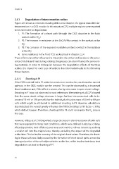
Figure 2.13 shows a schematic drawing of the cross-chapter of a typical monolithic in -
terconnection in a CIGS module. In this structure [27], multiple regions were reported
to be vulnerable to degradation:
1. P1: The formation of a shunt path through the CIGS absorber in the back
contact scribe (G )
sh
2. P2: The increase in resistance at the ZnO:Al/Mo contact in the contact scribe
(R )
c
3. P3: The corrosion of the exposed molybdenum back contact in the isolation
scribe (R )
s
4. Series resistance in the front TCO, as described in chapter 2.3.4
These effects can either influence the material in the scribe itself, or due to the occur-
rence of debris and heat during scribing, the process can also influence the surround-
ing materials. In order to distinguish between the degradation effects of the three
scribes, the impact for each type of scribe is described individually in the following
three chapters.
2.5.1.1 Shunting in P1
If the CIGS material in the P1 scribe becomes more conductive, an alternative current
pathway in the CIGS module can be created. This can be observed by a decreased
shunt resistance and, if the effect is severe, also by a decrease in open circuit voltage.
Shunting in P1 was not observed in most references: Wennerberg et al. [27] showed
that the open circuit voltage decrease is larger for four interconnected cells (a de-
crease of 75 mV or 13% per cell) than for individual cells (a decrease of 35 mV or 6% per
cell), which might be attributed to additional shunting in P1. However, calculations
also indicated this would greatly influence the fill factor (drop to fill factor < 30%),
which did not happen. Therefore, shunting in the P1 could not explain the V drop in
oc
this case.
However, Allsop et al. [110] reported a large decrease in shunt resistance of solar cells
that were exposed to damp heat conditions, which were defined in size by scribing.
After degradation, their efficiency was measured and the cell was remade by scribing
a smaller cell into the original area, thereby excluding the impact of the degraded
scribe lines. This led to the recovery of the original shunt values. Therefore, the shunt-
ing in these cells was likely caused by the formation of short circuit paths across the
damaged portion of the cell adjacent to the scribe line, which implies that damp heat
degradation can lead to shunting of P1.
78
2.5.1 Degradation of interconnection scribes
Figure 2.13 shows a schematic drawing of the cross-chapter of a typical monolithic in -
terconnection in a CIGS module. In this structure [27], multiple regions were reported
to be vulnerable to degradation:
1. P1: The formation of a shunt path through the CIGS absorber in the back
contact scribe (G )
sh
2. P2: The increase in resistance at the ZnO:Al/Mo contact in the contact scribe
(R )
c
3. P3: The corrosion of the exposed molybdenum back contact in the isolation
scribe (R )
s
4. Series resistance in the front TCO, as described in chapter 2.3.4
These effects can either influence the material in the scribe itself, or due to the occur-
rence of debris and heat during scribing, the process can also influence the surround-
ing materials. In order to distinguish between the degradation effects of the three
scribes, the impact for each type of scribe is described individually in the following
three chapters.
2.5.1.1 Shunting in P1
If the CIGS material in the P1 scribe becomes more conductive, an alternative current
pathway in the CIGS module can be created. This can be observed by a decreased
shunt resistance and, if the effect is severe, also by a decrease in open circuit voltage.
Shunting in P1 was not observed in most references: Wennerberg et al. [27] showed
that the open circuit voltage decrease is larger for four interconnected cells (a de-
crease of 75 mV or 13% per cell) than for individual cells (a decrease of 35 mV or 6% per
cell), which might be attributed to additional shunting in P1. However, calculations
also indicated this would greatly influence the fill factor (drop to fill factor < 30%),
which did not happen. Therefore, shunting in the P1 could not explain the V drop in
oc
this case.
However, Allsop et al. [110] reported a large decrease in shunt resistance of solar cells
that were exposed to damp heat conditions, which were defined in size by scribing.
After degradation, their efficiency was measured and the cell was remade by scribing
a smaller cell into the original area, thereby excluding the impact of the degraded
scribe lines. This led to the recovery of the original shunt values. Therefore, the shunt-
ing in these cells was likely caused by the formation of short circuit paths across the
damaged portion of the cell adjacent to the scribe line, which implies that damp heat
degradation can lead to shunting of P1.
78